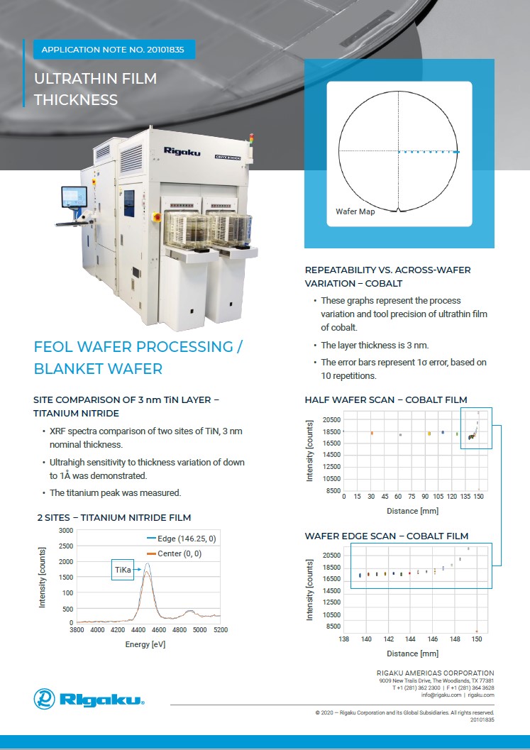
Rigaku Logo 100px

ONYX 3000

IN-LINE NON-DESTRUCTIVE WAFER INSPECTION AND METROLOGY

Hybrid configuration | automated x-ray analysis, 3D scanning, and 2D microscope for film thickness and composition measurements on blanket and patterned wafers

Wafer sizes

Is WAFER LEVEL PACKAGING an issue for your semiconductor manufacturing process?

EXPLORE ONYX 3000

< Click to play the video and view the ONYX 3000 in action. 

Hybrid configuration | automated x-ray analysis, 3D scanning, and 2D microscope for film thickness and composition measurements on blanket and patterned wafers.

Got questions?  Contact us for more information

CONTACT US

TECHNICAL SPECIFICATIONS

2D MICROSCOPE 

2d microscope features-1

2D MICROSCOPE MAGNIFICATION

2d microscope magnification

3D SCANNER

3d scanner features
Combining advanced X-ray and optical techniques, the ONYX 3000 offers a unique wafer metrology approach in many areas from FEOL through WLP, leading to in-line solutions for these processes. This sophisticated hybrid metrology tool enables high-throughput, in-line measurements on a blanket and product wafers ranging from ultra-thin single-layer films to multi-layer stacks.

The optical feature with 2D microscope and 3D scanner enables defect detection, sizing, and characterization of BEOL structures through image analysis (of critical dimensions, height, roughness, etc. of metal stacks, solder bumps, pillars, etc.) complemented by elemental composition and thickness measurements by ED-XRF analysis.

Hybrid configuration | automated x-ray analysis, 3D scanning, and 2D microscope for film stack, bumps and composition measurements on blanket and patterned wafers

Layer-by-layer wafer inspection with qualitative and quantitative results

  • XRF measures elemental composition and film thickness
  • 2D Microscope used for pattern recognition, CD calculation.
  • 3D Scanner height measurement, area scan, wafer surface roughness and bumps co-planarity
ONXY 3000 UNIQUE ADVANTAGES
  •  Optimal configuration for bumps inspection
  •  Array of 4 silicon drift detectors (SDD) with large active area and 123 eV FWHM (@5.9 keV) resolution
  • Measures light (low-energy) elements (carbon, oxygen, magnesium, aluminum, and phosphorous) using an optional helium atmosphere and special SDD detectors
  • Monochromatic or polychromatic x-ray options
  • Inspects micro-features through focused vertical X-ray beam (down to 10 µm diameter for polychromatic optics and 20 µm diameter for monochromatic optics)
  • Advanced motion platform for sub-micron accuracy
  • Precise 3D geometrical inspection of features: micro-bumps, pillars, and pads
  • Composition analysis associated with FinFET structures
  • Fully automated calibration processes, ensuring long-term stability and consistency, and tube aging correction
  • In line with SECS/GEM communication protocols

X-ray Optics Options

Polycapillary x-ray optics

Provide polychromatic and enhanced performance of XRF analysis to identify a wide range of elements efficiently

Monochromatic COLORS™-t x-ray optics

Enables measurements in low background spectrum enabling effective analysis of low signals.
• High brightness excitation
• Small spots for a wide range of thin film applications.
• Ideal configuration for bumps and copper pillars inspection

SYSTEM PARAMETERS

SPECIFICATIONS

Metrology Type

Micro-spot ED-XRF and optical inspection (2D-3D)

Wafer Size

Up to 300 mm

Wafer Type

Blanket and patterned wafers

X/Y Stage Resolution

< 1 µm (Stage resolution 0.1 µm)

Sample Handling

Magazine robot

Automation

Full wafer capability with single or dual automatic loader

Navigation

Precise stage complemented with an image recognition algorithm. Sub-micron fast navigation to single feature center.

SW User Interface

Auto calibration. Ease-of-use recipe creation and maintenance.Fundamental parameters optional.

Micro XRF beam Orientation

Vertical incidence micro-spot µXRF

X-ray tube energy

Up to 50 kV, 50 W

Optics

Polycapillary / COLORS™
(monochromatic x-ray optics)

Micro XRF beam Spot Size

10-50 µm spot sizes adjustable

Detector Type

Silicon drift detector (SDD) optional: light element detector (C,N,O,F.S)

Detector Resolution

123 ± 5 eV with a large solid angle

DPP | Digital Pulse Processor

High efficiency of more than 1 million photons/sec.

APPLICATIONS

Bump graph

SINGLE-BUMP METROLOGY

Measure and monitor Ag%, Sn%, Ni layers, Cu thickness, and total bump height:
  • Measure single-solder bumps as small as 10 μm diameter
  • Inspect a range of parameters: across the wafer, wafer-to-wafer, and lot-to-lot
  • Measure CD and a total height of single bumps using a 2D microscope, 3D scanner, and built-in sensors

THIN FILMS Measuring and monitoring

Measure and monitor thickness and composition of precious metal thin films:

  • Analyze ultra-thin films of any type of element, regardless of their physical properties


Thin film
UBM RDL

UBM/RDL

Conduct metallurgical inspections of under bump metallization (UBM) and redistribution layers (RDL):
  • Analyze multi-stack structures and thick monolayers, for layer thickness and composition
  • Distinguish separate layers simultaneously

ALLOY COMPOSITIONS

Measure and monitor metals and alloy composition:

  • Analyze metal elements (Ga, P, Co, Ni, Fe, Pt, Cr, Zn, and Mn)
  • Identify alloys (NiFe, CoNi, NiP, NiPt, and CrMn)

Alloy comp
Wafer metrology background drak grey

ONYX 3000 RESOURCES

TRUSTED PARTNER

WHO WE ARE
Pharmaceuticals have the power to change the world for the better, but before they can ever do that, they need to be proven safe and trustworthy. Here at Rigaku, we strive to make this a reality as the leading global scientific analytical instrumentation company specializing in X-ray and thermal analysis, and Raman spectroscopy.

CORPORATE MISSION
To contribute to the enhancement of humanity through scientific and technological development.

CORPORATE MOTTO
Value our customers, value our people, and value our technology